“Tomorrow will be another new materials world”
From the Stone Age to the present Silicon Era, civilization of man has been accomplished by the use of many new materials. Breakthrough in the growth of prospective materials and discovery of new functional materials are both important for the advancement of materials science and civilization. We aim to understand the Physics and Chemistry of materials synthesis that allow rational control of materials formation and their properties. Capabilities to control the growth and properties of materials are important for the realization of their applications in advanced electronic, photonic, chemical, electrochemical, and biological devices. We are dedicated in creating broader impact of new nanomaterials to people, environment, health, and renewable energy harvesting.
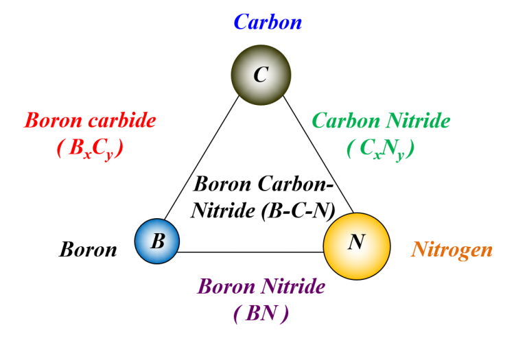
(I) Frontier Carbon Materials (B-C-N Nanostructures)
0D, 1D, and 2D Materials of
- Carbon (C): Nanotubes, graphene, nanoribbons, and new nanostructures
- Boron Nitride (BN): Nanotubes, BN Nanosheets (BNNSs), BN nanoribbons (BNNRs) and new nanostructures
- Boron Carbon-Nitride (BCN): Nanotubes, nanosheets, and new nanostructures
- Boron (B): Nanotubes, nanosheets, and new nanostructures
- Carbon Nitride (CN): New nanostructures
- B-C-N Hetero-Junctions and Hetero-structures: Graphene-BNNT junctions, BNNT/CNT junctions…
The arrangement of carbon atoms differentiates a pencil lead from a pricey jewel. Pencil lead consists of graphite where carbon atoms are sp2 hybridized for three covalent bonds . In diamonds, carbon atoms are sp3 hybridized for four bonds in a tetrahedral configuration. Graphite is soft, semi-metallic, and dark (zero energy band gap), while diamond is super-hard, insulating, and transparent (band gap = 5.4 eV). In the past three decades, new carbon materials like fullerenes, and carbon nanotubes (CNTs) have attracted tremendous research interest and have led to a Nobel Prize. Clearly, the change of bond hybridization and molecular packing among carbon atoms can make very exciting new materials.
Materials within the B-C-N triangular zone offer new vistas for materials research. They include thin films and nanostructures of carbon, or compounds constructed of multiple elements using B, C and N atoms: the smallest atoms that can form the strongest covalent bonds in solids. These materials are commonly called frontier carbon materials because of their flexibility to form various covalent bonds like those in pure carbon solids. Clearly, the ability to control bond hybridization, molecular packing, and composition of these materials is important to create new materials. They could possibly be useful for protective coatings, high-power electronics, and nanoscale devices: indispensable materials for the advancement of science in the new century.
In addition to investigating how to control the arrangement of B, C, and N atoms, the functions of kinetic energy of the growth species, potential energy of the growth species, and the role of catalysts in controlling bonding between B, C, and N atoms will be explored. The goal is to create new thin films and nanostructures of boron nitride, carbon nitride and boron-carbon-nitride with desired physical properties.
(II) Transition Metal Dichalcogenides (TMDCs)
Two-Dimensional Electronics and Optoelectronics: Present and Future
(III) Nanomaterials for Environmental, Health, and Energy Applications
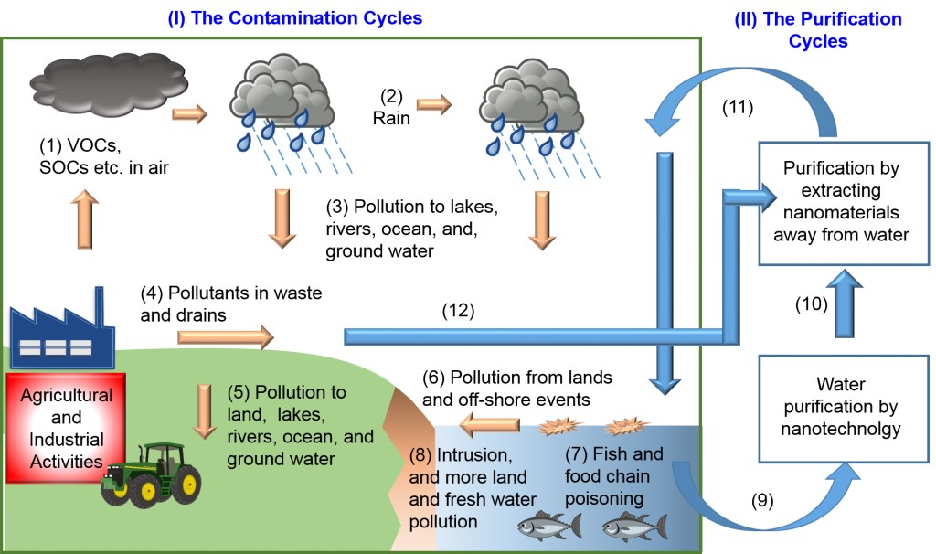
Organic pollutants from volatile organic compounds (VOCs), synthetic organic compounds (SOCs), oil spills, and waste disposal have significantly contaminated water and our food chain. The science and engineering of water purification, in particular oil–water separation, has attracted increasing attention in the past five years. As discussed in our review, both organic chemistry and nanotechnology have been employed for oil–water separation. This can be achieved using materials with specific wettability. On the other hand, the increased use of nanomaterials in water purification, sports equipment, and industrial and household products has raised concern about water contamination by nanoparticles. We are interested in water purification technology using nanomaterials as well as reclaim the nanomaterials from the purified water.